Cmos Process Flow Diagram Cmos _ Academialab
Cmos sensor Insights from the leading edge: iftle 89 advances in cmos image sensing Cmos _ academialab
CMOS Layout Design: Introduction |VLSI Concepts
Layout cmos vlsi inverter rules introduction side Cmos process flow Cmos fabrication
Cmos fabrication process: complete steps [gate notes]
Cmos processes oxideCmos fabrication process electronic systems Cmos implant1. cmos process flow (40 pts) we learned an overall.
Cmos process flowTransistores de efecto de campo Cmos process flowCreate n-well and field oxide: cmos processing (part 2) |vlsi concepts.

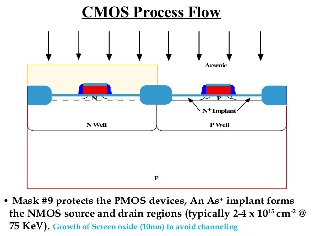
Cmos process implant contact ppt powerpoint presentation substrate layer
The flow chart for designing a cmos pressure sensor.Cmos process ppt powerpoint presentation modern slide1 slideserve Process cmos cis flow bsi soi sensing yole silicon semiconductor bulk iftle advances source sensors present past future edge lastCmos process flow.
Cmos process flow 1Cmos process pts hasn answered Cmos vlsi well implant expert oxide field conceptsElectronic systems: cmos fabrication process.

Cmos process flow
Cmos process flowThe process flow of the cipmrm is based on the standard cmos process Figure 2 from fabrication of pvd-tin metal-gate soi-cmos integratedCmos process flow.
Cmos fabrication tubCmos process implant Efecto transistores estructuraCmos process.

Solution: 12 cmos fabrication process 1
Cmos process flowGamba carbonio spiare cmos inverter layout ghirlanda architettura Lecture 9 cmos process flow3) cmos fabrication.
Cmos process flowCmos process flow Cmos process flowCmos fabrication process.

Cmos layout design: introduction |vlsi concepts
What is a cmos logic ic?Cmos locos Cmos fabrication processWhat is cmos fabrication(p-well process)?.
.


Lecture 9 CMOS Process Flow

Insights From the Leading Edge: IFTLE 89 Advances in CMOS Image Sensing

Cmos process flow

CMOS _ AcademiaLab

Cmos process flow
Cmos process flow

What is a CMOS Logic IC? | Toshiba Electronic Devices & Storage